

Circuit board
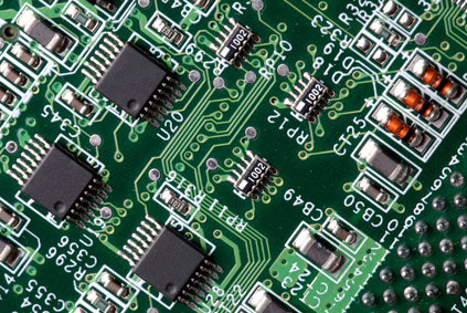
Circuit board
Layouts
We require the following documentation for layout design:
- Bills of materials
- Circuit diagrams
Circuit board production
Our technical capabilities include
- Single-layer, double-layer, multi-layer,
aluminium (metal core laminate) - CEM1, FR3, FR4 and FR5
| Material thickness | 0,55 mm to 3,2 mm |
| Cu layers | 18, 35, 70, 105 and 210 µm |
| Maximum dimensions | 500 mm x 600 mm |
| Track width and insulation | 120 µm |
| Minimum aperture diameter | 0,2 mm |
| Surface treatment | HAL lead-free (LF) OSP (organic surface protection) Au (electroless nickel or galvanic gold ) Ag (electroless silver) Sn (electroless tin) Graphite (carbon paste) |
| Solder mask | Green, black, white, blue or red |
| Service printing | White, yellow or black |
| Processing | Cutting, scribing, milling |
| Data formats | Gerber 274X CAM 350 Version 6 and later EAGLE 3.55 and later |
| Drill formats | Sieb & Mayer Excellon |